- 您现在的位置:买卖IC网 > Sheet目录366 > TPS23757EVM (Texas Instruments)EVALUATION MODULE FOR TPS23757
TPS23757
SLVS948D – JULY 2009 – REVISED NOVEMBER 2013
www.ti.com
(a)
t RECHARGE =
(C VC1 +C VC2 ) ′ V CUVH
I VC
(10 m F + 0.47 m F) ′ 3.5 V
= = 9.2 ms
4 mA
t DISCHARGE = = = 6.5 ms
t DISCHARGE 6.5 ms
(b)
(c)
(d)
(C VC1 +C VC2 ) ′ V CUVH (10 m F + 0.47 m F) ′ 3.5 V
I TOTAL 5.6 mA
(a) Note that the optocoupler current is 0 mA because the output is in current limit.
(b) Also, it is assumed I APb is 0 mA.
Duty Cycle: D = = = 41%
t DISCHARGE + t RECHARGE 6.5 ms + 9.2 ms
1 1
Hiccup Frequency: F = = = 64 Hz
t DISCHARGE + t RECHARGE 6.5 ms + 9.2 ms
6. The voltage rating of C VC1 and C VC2 should be 16 V minimum.
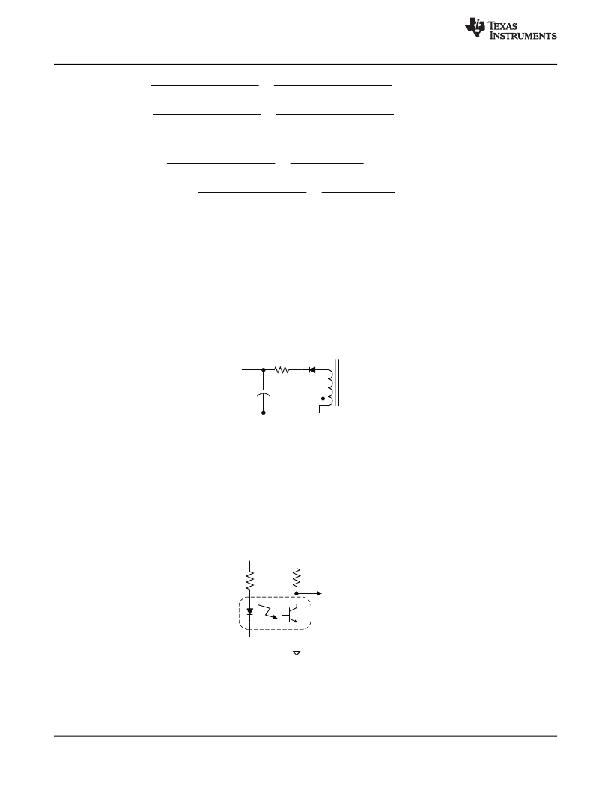
Switching Transformer Considerations and R VC
Care in design of the transformer and V C bias circuit is required to obtain hiccup overload protection. Leading-
edge voltage overshoot on the bias winding may cause V C to peak-charge, preventing the expected tracking with
output voltage. Some method of controlling this is usually required. This may be as simple as a series resistor, or
an R-C filter in front of D VC1 . Good transformer bias-to-output-winding coupling results in reduced overshoot and
better voltage tracking.
R VC as shown in Figure 27 helps to reduce peak charging from the bias winding. This becomes especially
important when tuning hiccup mode operation during output overload. Typical values for R VC will be between 10
? and 100 ? .
V C
R VC
D VC1
T1
Bias Winding
ARTN
Figure 27. R VC Usage
APb Pin Interface
The APb pin is an active low, open-drain output indicating an adapter power source is available. An optocoupler
is typically used to interface with the APb pin to signal equipment on the secondary side of the converter of APb
status. Optocoupler current-gain is referred to as CTR (current transfer ratio), which is the ratio of transistor
collector current to LED current. To preserve efficiency, a high-gain optocoupler ( 250% ≤ CTR ≤ 500%, or 300%
≤ CTR ≤ 600% ) along with a high-impedance (e.g., CMOS) receiver are recommended. Design of the APb
optocoupler interface can be accomplished as follows:
V C
R APb
V OUT
R APb_OUT
Adapter Present
Indicator
Low = Present
APb From
TPS23757
Figure 28. APb Interface
1. APb ON characteristic: I APb = 2 mA minimum, V APb = 1 V
2. Let V C = 12 V, V OUT = 5 V, R APb-OUT = 10 k ? , V APb-OUT (low) = 400 mV max
28
Submit Documentation Feedback
Copyright ? 2009–2013, Texas Instruments Incorporated
发布紧急采购,3分钟左右您将得到回复。
相关PDF资料
TPS62230EVM-370
EVAL MODULE FOR TPS62230-370
TRAVELCUBE
SURGE SUP 1OUT W/RJ11 DIRECTPLUG
TRAVELER100BT
SURGE SUP 2OUT W/RJ11 DIRECTPLUG
TRAVELER3USB
SURGE SUPP USB CHARGE TRAVEL SZ
TRAVELERC6
SURGE SUPPRESSOR 120/240V RJ11
TRAVELERC8
SURGE SUPPRESSOR 120/240V RJ11
TRAVELER
SURGE SUP 2OUT W/RJ11 DIRECTPLUG
TRK-MPC5604B
MPC5604B 144PIN REV 2.1
相关代理商/技术参数
TPS23757PW
功能描述:热插拔功率分布 Hi Eff PoE Inter & DC/DC Controller RoHS:否 制造商:Texas Instruments 产品:Controllers & Switches 电流限制: 电源电压-最大:7 V 电源电压-最小:- 0.3 V 工作温度范围: 功率耗散: 安装风格:SMD/SMT 封装 / 箱体:MSOP-8 封装:Tube
TPS23757PWR
功能描述:热插拔功率分布 Hi Eff PoE Interface & DC/DC Controller RoHS:否 制造商:Texas Instruments 产品:Controllers & Switches 电流限制: 电源电压-最大:7 V 电源电压-最小:- 0.3 V 工作温度范围: 功率耗散: 安装风格:SMD/SMT 封装 / 箱体:MSOP-8 封装:Tube
TPS2375D
功能描述:热插拔功率分布 IEEE 802.3af PoE Pwr Device Cntrler RoHS:否 制造商:Texas Instruments 产品:Controllers & Switches 电流限制: 电源电压-最大:7 V 电源电压-最小:- 0.3 V 工作温度范围: 功率耗散: 安装风格:SMD/SMT 封装 / 箱体:MSOP-8 封装:Tube
TPS2375D
制造商:Texas Instruments 功能描述:POWER OVER ETHERNET ((NW))
TPS2375DG4
功能描述:热插拔功率分布 IEEE 802.3af PoE Pwr Device Cntrler RoHS:否 制造商:Texas Instruments 产品:Controllers & Switches 电流限制: 电源电压-最大:7 V 电源电压-最小:- 0.3 V 工作温度范围: 功率耗散: 安装风格:SMD/SMT 封装 / 箱体:MSOP-8 封装:Tube
TPS2375DR
功能描述:热插拔功率分布 IEEE 802.3af PoE Pwr Device Cntrler RoHS:否 制造商:Texas Instruments 产品:Controllers & Switches 电流限制: 电源电压-最大:7 V 电源电压-最小:- 0.3 V 工作温度范围: 功率耗散: 安装风格:SMD/SMT 封装 / 箱体:MSOP-8 封装:Tube
TPS2375DRG4
功能描述:热插拔功率分布 IEEE 802.3af PoE Pwr Device Cntrler RoHS:否 制造商:Texas Instruments 产品:Controllers & Switches 电流限制: 电源电压-最大:7 V 电源电压-最小:- 0.3 V 工作温度范围: 功率耗散: 安装风格:SMD/SMT 封装 / 箱体:MSOP-8 封装:Tube
TPS2375EVM
功能描述:电源管理IC开发工具 TPS2375 POE Powed Device Eval Mod RoHS:否 制造商:Maxim Integrated 产品:Evaluation Kits 类型:Battery Management 工具用于评估:MAX17710GB 输入电压: 输出电压:1.8 V
